DC–DC Buck Converter for Solar Car Competition
Summary
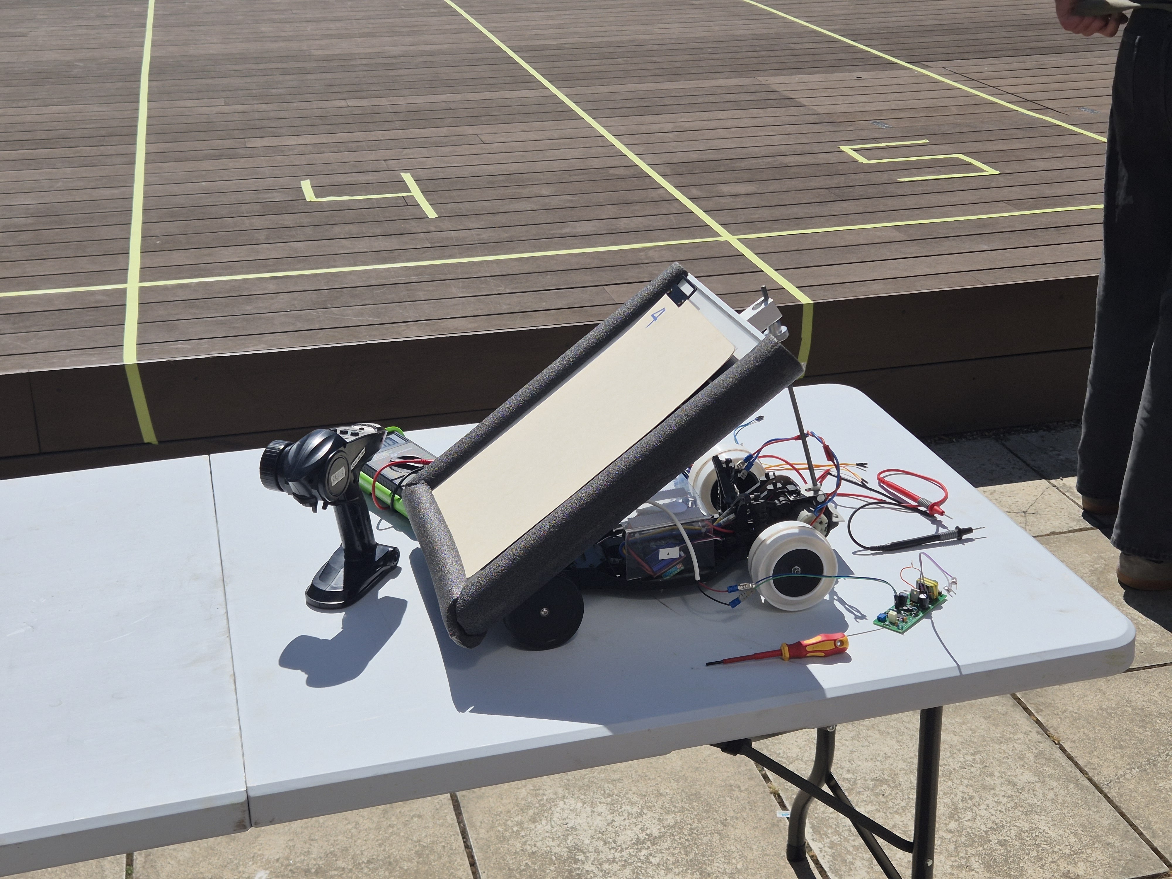
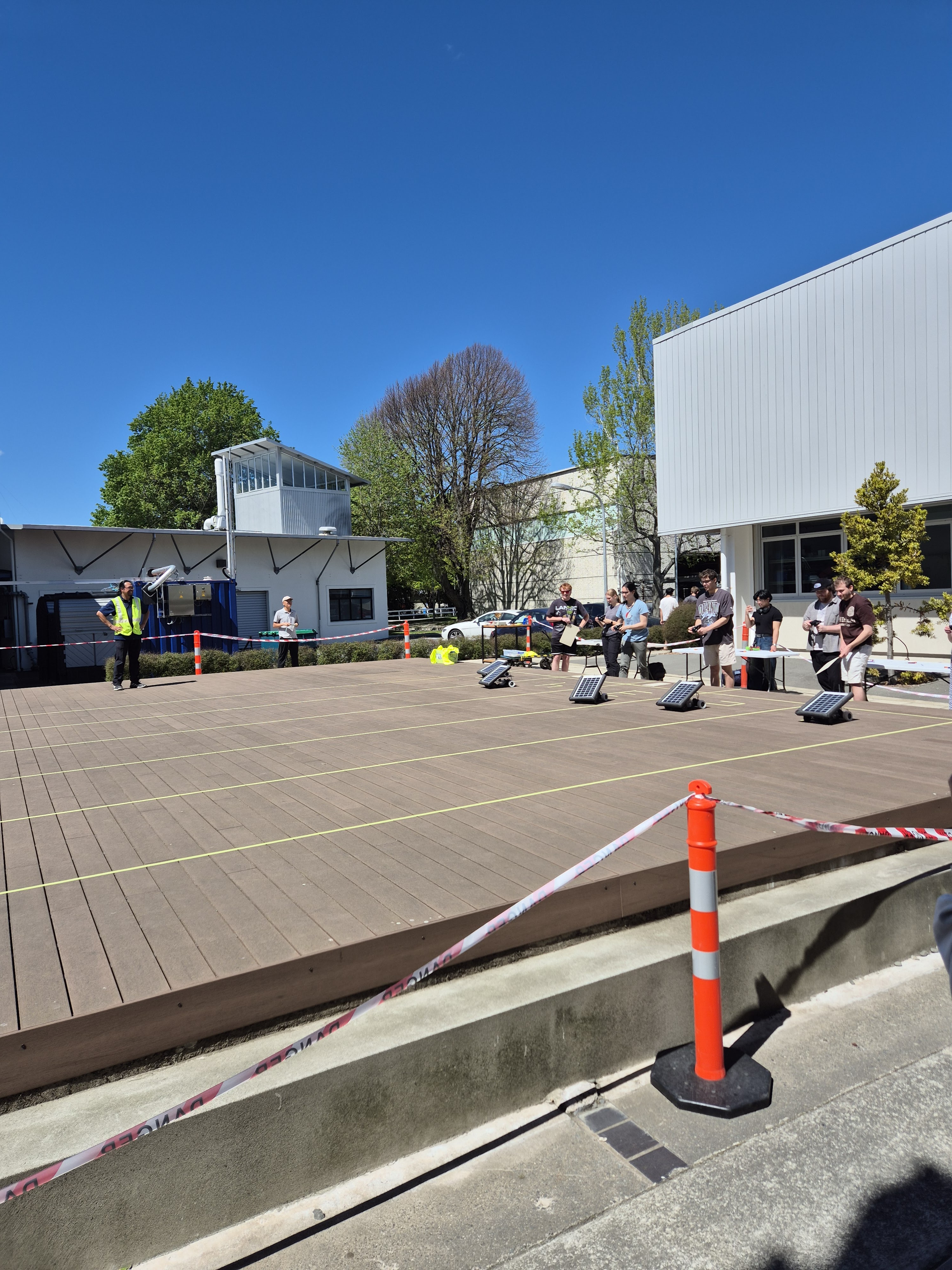
Designed, simulated, and built a DC–DC buck converter to power a model solar car directly from a 10 W solar panel for a university competition (team of 3). The goal was to regulate a variable renewable source and keep the panel operating near its maximum power point while delivering stable power to a DC motor. I led the analytical design, LTspice simulation, inductor design and construction, TL494-based control implementation, and PCB layout. The final converter operated in continuous conduction at 51.3 kHz and successfully powered the car under changing light and load conditions. Moving from breadboard to PCB significantly improved stability and switching performance.
More Information About the Project
This project required designing a switching power converter from first principles rather than using an off-the-shelf module. The solar panel voltage varied with light intensity and motor load, meaning the converter had to both regulate output voltage and prevent the panel from being pulled away from its optimal operating point.
Engineering Design Approach
I began with worst-case analytical sizing to ensure continuous conduction and controlled ripple. Initial calculations were validated and refined using LTspice simulation. Simulation results showed that increasing inductance from 100 μH to ~200 μH reduced ripple and improved stability, so I adjusted the design accordingly before hardware build.
Inductor Design and Construction
The final inductor was designed and hand-wound on an RM8 core:
- Designed turns and air gap from flux density limits
- Measured final inductance: 208 μH (within 4% of target)
- Confirmed continuous conduction through measured waveforms
Control and Power Stage Decisions
The TL494 PWM controller was configured for ~50 kHz switching (measured 51.3 kHz). Development was staged to reduce risk:
- Open-loop testing to validate switching behaviour
- Closed-loop voltage feedback to maintain panel operation near its maximum power point (14–16 V depending on light conditions)
Integral control was implemented to stabilise the response while avoiding oscillations caused by mechanical vibration and rapid switching transients.
During testing, the TL494 output drive was insufficient to fully saturate the MOSFET. I designed and implemented a BJT push-pull gate driver stage to increase drive current. Oscilloscope measurements confirmed proper gate voltage and clean switching behaviour. This highlighted a key practical lesson: control IC outputs often require buffering when driving power-stage devices.
PCB Design and Practical Improvements
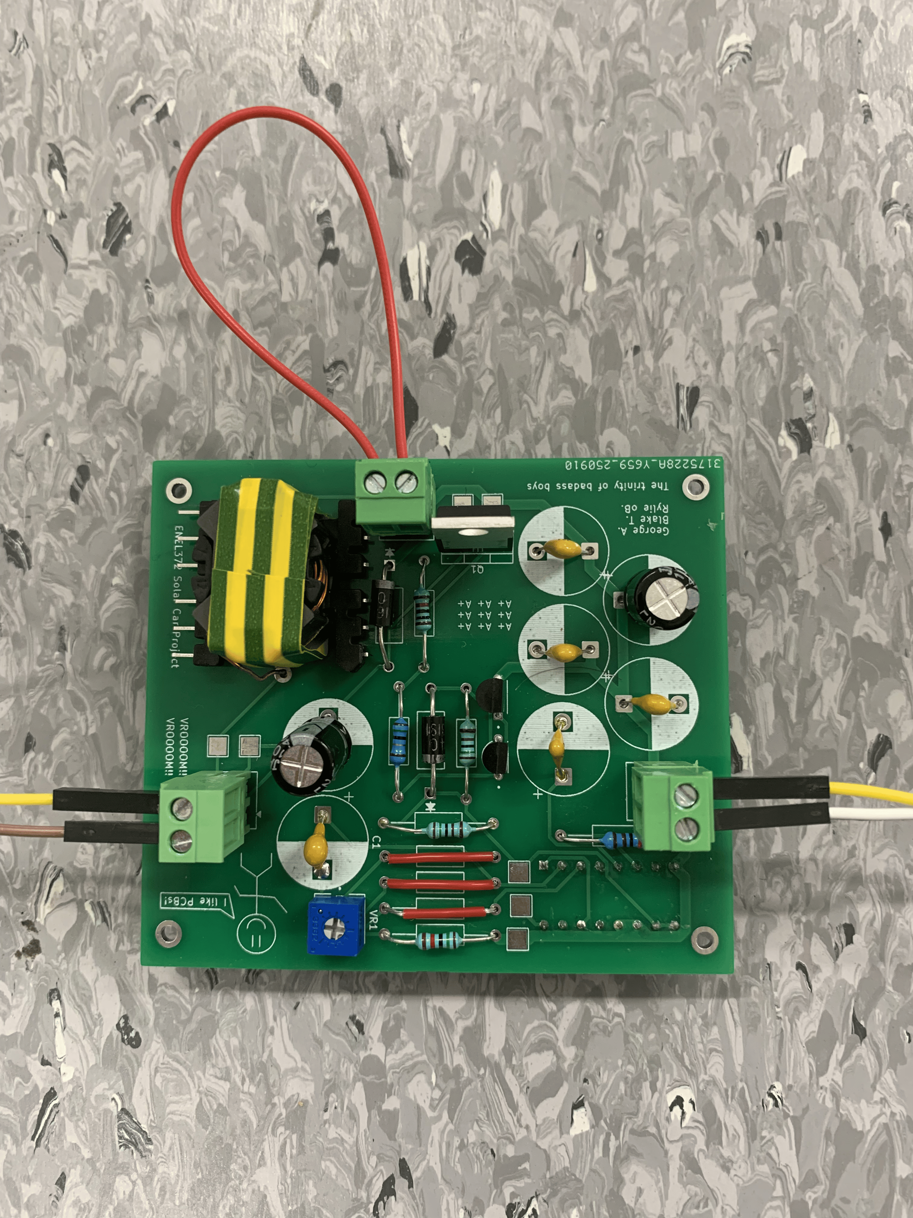
Initial breadboard testing showed unstable behaviour caused by parasitic inductance and long switching loops. I redesigned the system onto a PCB with a ground plane, short high-current paths, careful decoupling placement, and wider power traces. The PCB significantly improved waveform clarity and reduced switching noise.
A layout error (incorrect TL494 footprint orientation) was identified during bring-up due to abnormal current draw and heating. The issue was diagnosed and corrected quickly, reinforcing the importance of hardware validation and a systematic debugging process.
Performance Outcome
- Measured switching frequency: 51.3 kHz (close to 50 kHz design)
- Continuous inductor current operation
- Stable motor startup and steady-state behaviour
- Closed-loop control maintained panel near MPP under varying light
- Measured ripple was higher than simulation due to motor commutation noise, highlighting the difference between ideal resistive models and real inductive loads
Artifacts
Key skills & tools
Power Electronics
- Buck converter design (continuous conduction mode)
- Magnetic component design and hand-winding (RM8 core)
- MOSFET switching and gate driver design
- Renewable source integration (solar panel behaviour)
Control & Simulation
- TL494 PWM configuration
- Closed-loop voltage feedback implementation
- Integral control tuning
- LTspice circuit simulation and waveform analysis
Hardware & PCB
- KiCad schematic capture and PCB layout
- Ground plane and loop-area optimisation
- Decoupling and noise mitigation strategies
- Oscilloscope-based validation and hardware debugging
Gallery